
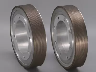
CMP Conditioner for dressing polishing pad in semiconductor industry
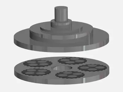
What is CMP Pad Conditioner ?
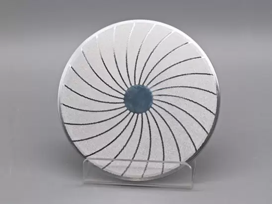
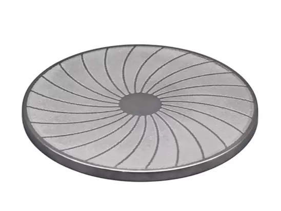
CMP Pad Conditioner uses advanced diamond planting technology to fix diamond abrasive grains on the substrate in an orderly manner according to the designed pattern. It uses precision electroplating to match diamonds of different sizes, shapes, and pattern designs to provide different A series of polishing pad removal rate products can be widely used in various scenarios that require planarization.
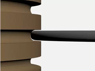
When the feature size of a semiconductor chip is less than 0.35μm, global planarization must be performed. CMP is currently the only global planarization technology. The polishing fluid used by CMP is composed of chemical components and submicron or nanometer abrasives and removes processed materials through a combination of chemical corrosion and mechanical force. The polishing pad is in direct contact with the polishing fluid and the wafer. The grooves on the surface of the polishing pad play a role in distributing the polishing fluid and removing waste fluid. The surface roughness and flatness of the polishing pad directly affect the results of CMP.
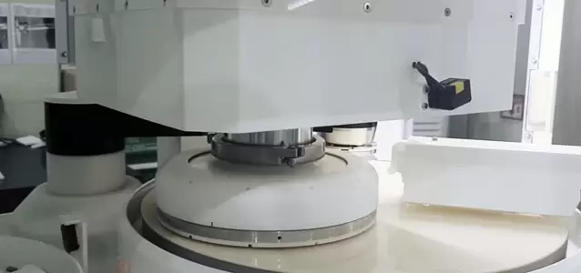
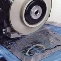
The polishing pad is prone to aging and surface grooves are easily clogged during CMP processing, causing the polishing pad to lose its polishing effect. At this time, a diamond dresser is required to trim the surface of the polishing pad. The CMP Pad Conditioner has the role of removing waste liquid in the groove of the polishing pad, improving the surface roughness of the polishing pad and improving the flatness of the polishing pad. Therefore, the performance of the CMP pad conditioner directly affects the global planarization effect of the wafer surface.
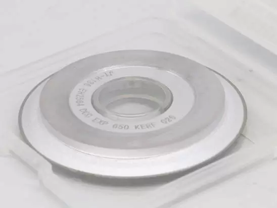
CMP Pad Conditioner, also known as CMP dresser, mostly uses a metal matrix and combines diamond abrasive grains with the matrix through high-temperature brazing technology. The CMP dresser has the functions of removing groove waste liquid, extending the service life of the polishing pad, and improving the flatness of the polishing pad. Its performance will directly affect the wafer planarization effect.
When the feature size of a semiconductor chip is less than 0.35μm, global planarization is required, and CMP (Chemical Mechanical Polishing) is currently the only global planarization technology. The CMP polishing pad is a key consumable for wafer planarization. During use, the CMP polishing pad has problems such as easy aging and easy clogging of surface grooves. In order to ensure polishing efficiency and accuracy, the CMP polishing pad requires a CMP pad conditioner for processing.
What are the applications of CMP-Disk?
1. Semiconductor CMP process
2. Silicon wafer polishing process
3. Polishing of third-generation semiconductors such as silicon carbide
4. Sapphire polishing
In the front-end processing steps of semiconductors, the uses of diamond tools include the following:
Cutting:
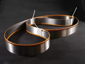
Cutting including crystal ingot cutting and slicing. Electroplated diamond band saws or inner circle cutting discs can be used to cut crystal ingots. However, inner circle or outer circle cutting has low efficiency, high material loss rate, and low processing quality. Therefore, diamond band saws are currently used to cut crystal ingots. The methods for slicing ingots mainly include internal circular cutting and wire cutting. Compared with internal circular cutting, wire cutting has the advantages of high efficiency, large cutting diameter and small saw mark loss. Currently, silicon-based semiconductors mainly use abrasive wire saw cutting processing.
Grinding and polishing
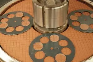
Including crystal rod rolling, wafer surface grinding, wafer edge chamfering and edge grinding. Different grinding areas require different grinding wheel shapes and thicknesses and other parameters. CMP dresser’s current 300mm silicon wafer size has become the international mainstream, and 450mm silicon wafers are also under development. The area of a 300mm diameter silicon wafer is 2.25 times that of 200mm, and the number of chips it can produce is 144 more than that of 200mm. The increase in wafer size can double the production efficiency of enterprises, but on the other hand, the increase in wafer size will place higher demands on diamond tools.
Chemical mechanical polishing (CMP) technology is one of the key technologies for surface processing of semiconductor wafers and is used for surface planarization at various stages of the integrated circuit manufacturing process. It has been widely used in recent years. During the CMP process, the polishing pad has the functions of storing and transporting polishing fluid, removing processing residual materials, transmitting mechanical loads, and maintaining the polishing environment. As the CMP process continues, the physical and chemical properties of the polishing pad will change, which is manifested as residual substances on the surface of the polishing pad, the volume and number of micropores are reduced, the surface roughness is reduced, and molecular reorganization occurs on the surface, forming a certain The thickness of the glaze layer leads to a reduction in polishing efficiency and polishing quality. In order to eliminate the above phenomenon, the polishing pad must be trimmed. Reasonable trimming can not only improve the polishing effect, but also extend its service life and reduce polishing costs.
(3) When the characteristic size of the semiconductor chip is less than 0.35μm, global planarization must be performed. CMP is currently the only global planarization technology. The polishing fluid used by CMP is composed of chemical components and submicron or nanometer abrasives, and removes processed materials through a combination of chemical corrosion and mechanical force. CMP dressers generally use a metal matrix and combine diamond abrasive grains with the matrix through high-temperature brazing technology. A CMP dresser with excellent performance should have the characteristics of high material removal rate, diamond abrasive grains that are not easy to fall off, equal height and uniform distribution, so as to ensure that the wafer can achieve qualified global planarization. Backside thinning grinding wheel Thinning grinding wheel plays an important role in the chip preparation process: First, the thinning process can reduce the overall thickness of the chip, which is beneficial to heat dissipation and integration. The second is to reduce the thickness and surface roughness of the damage layer on the wafer surface, release the internal stress caused by the various processes before thinning, and reduce the degree of collapse of a single chip during the dicing process.
Wafer thinning generally uses wafer rotation grinding, and the processing process includes rough grinding and fine grinding. The axial feed speed of rough grinding is high, and a diamond grinding wheel with a larger particle size is used to quickly remove about 90% of the machining allowance; the axial feed speed of fine grinding is low, and a diamond grinding wheel with extremely small particle size is used.
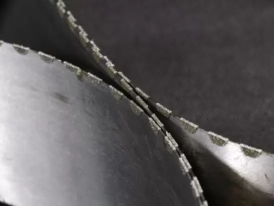
Dicing blade can be divided into hubless and hub-type according to the installation method. Dicing is the last step in wafer processing, and the quality of the dicing knife will directly affect the quality of a single chip. Semiconductor materials are typical hard and brittle materials with high hardness, high brittleness, and low fracture toughness. The most important problem during dicing is cracking. Once cracking occurs, the chip will be scrapped and the entire processing process will fail.
There are three main factors that affect the processing quality of the dicing blade:
Diamond particle size, diamond density, bond strength.
The diamond particle size is small, the dicing knife has good self-sharpening properties, and the wafer will not crack after sharp cutting, but the processing efficiency is low and the service life is short; the diamond particle size is large, the processing efficiency is high, the service life is long, but the processing quality is poor. The density of diamond is high, and the load resistance of the dicing blade is poor, and the wafer will crack greatly after cutting, but the life is long; the density of diamond is small, the load resistance of the dicing blade is increased, and the processing quality is high, but the life is shortened. The strength of the bond is low, and the tool can maintain good self-sharpening and high processing quality, but its service life is short; the strength of the bond is high, and the service life of the tool is long, but it is easily damaged when cutting hard materials, and the processing quality is not as good as that of the height of hubless bond dicing blade.
—EDITOR: Doris Hu
—POST: Doris Hu