
The key materials used for semiconductor advanced packaging and testing
Packaging is one of the downstream processes in semiconductor wafer manufacturing. Its purpose is to support and protect the chip, connect the chip to external circuits, and enhance thermal conductivity.
The development of packaging technology is accompanied by the continuous improvement of chip performance, continuous miniaturization of size, and continuous breakthroughs in technology to meet the growing chip needs.
Semiconductor devices have many packaging forms. According to the shape, size and structure of the package, they can be divided into three categories: pin insertion type, surface mount type and advanced packaging. From DIP, SOP, QFP, PGA, BGA to CSP and then to SIP, the technical indicators are more advanced than the previous generation.
Epoxy molding compound is an important microelectronic packaging material and one of the main materials that determines the final packaging performance. It has the advantages of low cost and high production efficiency. It has become an indispensable and important material for semiconductor packaging.
Epoxy Molding Compound(Epoxy Molding Compound, referred to as EMC) is a thermosetting chemical material used for semiconductor packaging. It is composed of epoxy resin as matrix resin, high performance phenolic resin as curing agent, and silicon powder as filler. As well as the addition of a variety of additives mixed into the powder molding plastic, as one of the main raw materials of the packaging, epoxy plastic encapsulation material can be applied to integrated circuits, discrete devices and other semiconductor packaging, at present more than 95% of microelectronics devices are epoxy plastic encapsulation devices, more than 90% of integrated circuits are using epoxy plastic encapsulation material, therefore, Epoxy plastic sealant has become a key supporting industry for the development of semiconductor industry. Epoxy plastic sealing material has the function of protecting the chip from the external environment, resisting external solvents, moisture, impact, and ensuring the electrical insulation between the chip and the external environment.
Several important properties of epoxy molding compounds have an impact on semiconductor packaging:
(1) The impact of the dielectric properties of epoxy molding compounds on semiconductor packaging
Dielectric properties include the dielectric constant, dielectric loss, conductivity and volume resistivity of the material, which are important parameters that characterize the insulation or conductivity of the material itself. Since epoxy molding compounds are mixed, melted and kneaded from a variety of components during the manufacturing process, the dielectric properties of each component themselves vary greatly, resulting in different epoxy molding compounds having different dielectric properties due to different formulas. There is a big difference in performance. Since epoxy molding compound mainly plays the role of insulator in semiconductor packaging, its dielectric properties will have an important impact on the electrical properties of the packaged semiconductor device. Especially for the packaging of high-voltage devices, epoxy molding compound is required. Relatively low dielectric constant and loss as well as large volume resistivity within a certain temperature range usually require specific formula adjustments to be achieved. Generally speaking, the dielectric properties of epoxy molding compounds can be improved by selecting less polar raw materials and controlling the purity of the raw materials.
(2) The effect of water absorption of epoxy molding compound on semiconductor packaging
The water absorption rate of epoxy molding compounds is another important indicator to measure the performance of epoxy molding compounds. Since cross-linked epoxy resin has no sealing effect on water molecules, under certain ambient humidity and temperature, water molecules can diffuse from the outside through the molding compound into the packaged device, causing damage to the packaged device. This damage is not only reflected in the reduction of interface strength and the formation of vapor pressure at instantaneous high temperatures, causing internal delamination of the device, but also water molecules can serve as carriers of impurity ions in the molding compound, bringing impurity ions to the chip surface and pad surface, thereby causing Different degrees of corrosion and surface charge deposition seriously affect the electrical performance of packaged devices. Therefore, reducing the water absorption rate of materials is always an important direction to improve the performance of epoxy molding compounds.
(3) The influence of the stress of epoxy molding compound on semiconductor packaging
The stress of epoxy molding compound is another important factor in measuring the performance of epoxy molding compound. Its size mainly depends on the thermal expansion coefficient and modulus of epoxy molding compound.
Since the thermal expansion coefficient and modulus of different raw materials are different, the thermal expansion coefficient and modulus of epoxy molding compound can be controlled and adjusted by controlling the proportion of raw material types to achieve the purpose of adjusting stress. In semiconductor packaging, the thermal expansion coefficient of epoxy molding compound is much larger than other inorganic packaging materials such as chips, frames, and base islands. As the temperature changes, thermal stress occurs at the material interface due to the mismatch in thermal expansion coefficients of different materials in the packaged device. If this stress is greater than the adhesion force of the corresponding interface, it will cause delamination of the interface and even cause cracking of the entire package.
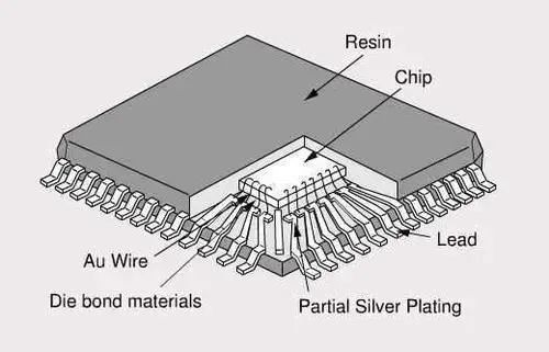
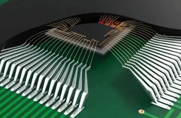
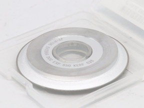
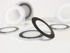
Package lead frames (one of which mainly refers to copper alloy lead frames; There is also a main talk about the QFN package lead frame is mainly focused on wage solutions), the lead frame is mainly composed of two parts: chip solder plate (die paddle) and lead finger. As the chip carrier of the integrated circuit, the lead frame is a key structural part of the electrical circuit circuit of the chip (bonding point) through the electrical connection between the internal lead and the external lead by means of bonding materials (gold wire, aluminum wire, copper wire), which forms the electrical circuit. At present, the widely used copper alloys are: copper-iron-phosphorus, copper-nickel-silicon, copper-chromium-zirconium, copper-silver, copper-tin and other alloy systems; The ideal lead frame material is a high-conductivity, high-strength, high-function material with tensile strength above 600MPa, electrical conductivity above 80%, and anti-softening temperature greater than 500℃.The welding process uses tin powder solder paste (solder paste is a process that has gradually emerged in the field of IGBT packaging in recent years), the solder paste is made of high lead alloy, which can be used in the field of semiconductor packaging and welding, for the packaging of electronic components and chip ics, and can also be used in other metal welding requiring high temperature solder. The welding performance of superalloy solder paste is stable and the cavity rate is less than 5%.
The new welding thermal interface material can greatly reduce the contact thermal resistance and increase the heat transfer efficiency by filling the gap between the heat source and the heat dissipation unit of the device through the thermal interface material. Mainly solve the problem of heat dissipation management of chip packaging.
Advanced sealing and loading plate, that is, we usually say packaging substrate, courseware mentioned advanced packaging Chiplet FCBGA, at that time do not care what Chiplet. Check Chiplet commonly known as core, also called small chip, it is a class of die(nude) to meet specific functions, Through die-to-die internal interconnection technology, multiple module chips and the underlying chip are packaged together to form a system chip, so as to realize a new form of IP reuse. I understand that Chiplet should be a small chip technology, through chiplet technology, a single chip area will be greatly reduced, the yield can be greatly improved, thereby reducing the mass production cost of the chip, improve the reliability of the chip, to achieve the overall cost reduction and efficiency.
Power semiconductor packaging paste (power semiconductor chip packaging sintered silver, ceramic copper clad plate brazing paste, etc.)
Why need back grinding?
The thickness of silicon wafers for semiconductor integrated circuits is 520 μm for 4 inches and 670 μm for 6 inches. This brings difficulty to the chip slicing. Therefore, after the circuit layer is produced, the back side of the silicon wafer needs to be thinned to the required thickness, and then diced to form thinned bare chips one by one.
1. Back Thinning process
Silicon wafer backside thinning technologies mainly include:
Grinding, grinding, chemical polishing, dry polishing, electrochemical corrosion, wet corrosion, plasma enhanced chemical corrosion, atmospheric pressure plasma corrosion, etc.
Thick silicon wafers are glued onto a thin film (often called blue film) with a metal ring or plastic frame and sent to a dicing machine for scribing. Nowadays, they are all automatic dicing machines, equipped with laser or diamond dicing tools. Cutting is divided into partial scribing (not scribing to the bottom, leaving residual thickness) and complete dividing and scribing. For partial scribing, use an ejection pin to force the chips completely apart. When scribing, there will be more or less microcracks and grooves on the edge, depending on the sharpness of the tool. This will seriously affect the chip’s chip strength.
This study is also a field of deep digging and extension, need to slowly digest, packaging is an important step during the semiconductor process, also involves the packaging grinding products used, Moresuperhard have many customers in the the current packaging grinding, and cutting but also need to expand.
Silicon carbide module packaging new materials, Sumitomo Bakaki mentioned the development process of the power module (silicon carbide power module production process mainly includes ceramic substrate sheet, silver paste printing, chip patch, silver sintering, vacuum reflow, lead frame assembly welding, lead bonding, plasma cleaning, plastic sealing, X-ray detection, test packaging and other links. The challenge of SIC plastic sealing module and the difference between traditional pot-sealing modules and the requirements of sic wafer for PBO positive photoadhesive are also mentioned again.
—-EDITOR: Doris Hu, Julia Zhang
—POST: Doris Hu, Julia Zhang