
How to high precision back grinding wafer ?
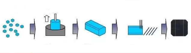
The raw material of a wafer is silicon, and there is an inexhaustible supply of silica on the surface of the earth’s crust. Silica ore is extracted by electric arc furnace, chlorinated by hydrochloric acid, and distilled into high purity polysilicon, its purity up to 99.999999999%.
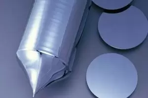
Purified, high-purity polysilicon is grown by spinning on a seed. After the polycrystalline silicon is melted, it is put into a Crucible, and then the daughter crystals are put into the Crucible at a uniform speed and pulled upward. Then the fused silicon will grow into a cylindrical ingot along the daughter crystals, and then the silicon ingot is cut into silicon wafers. Silicon ingots are then sliced, rolled, sliced, chamfered, polished and etched so that they have independent electrical properties and become the basic raw material of integrated circuit factories: silicon wafers, known as “wafers”.
Application of wafer:
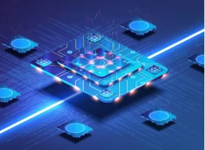
The packaged wafer is called an integrated circuit. At present, integrated circuits in information, communication, consumer electronics, automotive electronics, intelligent driving, aerospace, medical electronics and other consumer fields are expanding and growing, all electronic products involving circuits will use integrated circuits.
Wafers are the basic raw material for making semiconductor devices. High purity semiconductor through drawing, slicing and other processes to prepare wafer, wafer through a series of semiconductor manufacturing processes to form a very small circuit structure, and then cut, packaging, testing into chips, widely used in all kinds of electronic equipment.
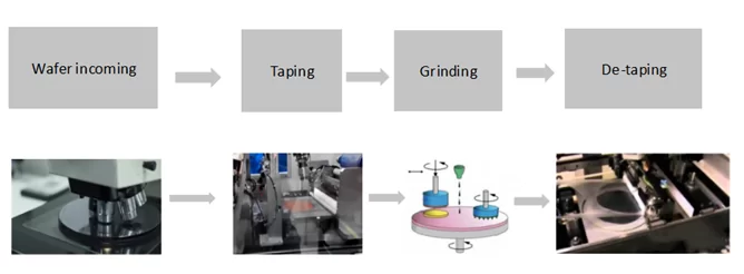
Wafer back grinding
Wafer back grinding is a step in semiconductor device manufacturing in which wafer thickness is reduced to allow stacking and high-density packaging of integrated circuits.
Integrated circuits are produced on semiconductor wafers and go through a series of processing steps. The thinner the semiconductor chip, the higher the chip stack, the higher the integration.
Wafer back grinding quality requirements:
1) Wafer integrity (no damage)
2) Wafer thickness accuracy and ultra-thin capacity requirements
3) Wafer TTV value requirements per second
4) Wafer surface roughness requirements
5) Wafer surface damage layer thickness (SSD) requirements
6) Wafer thickness consistency requirements
The most common thinning technique is wafer thinning grinding.
The grinding process can be divided into three stages:
The first step(rough grinding): using diamond back griding wheel with large grit, the grinding wheel feed per revolution is large, the cutting depth of a single abrasive grain is greater than the critical cutting depth. Is a typical brittle zone grinding. Relatively large feed speed is adopted to improve processing efficiency. This stage accounts for about 94% of the total thinning. This process can cause significant lattice damage and edge breakage.
The second step(fine grinding): the back grinding wheel is used, the feeding amount of grinding wheel per revolution is very small, and the cutting depth of some grinding grains is less than the critical cutting depth, which belongs to the ductility domain cutting. The other part of the cutting depth is greater than the critical cutting depth, belonging to the brittle region cutting. The lower feed speed can eliminate the damage and edge collapse caused by rough grinding at the front end. 6% of the total amount of grinding.
Third step(polishing): the last few microns using fine grinding polishing, grinding depth is less than 0.1μm, has entered the ductility domain processing range, at this time the material processing performance is the first deformation, and then tear the way of chemical change.
Wafer back grinding has the following advantages for chips:
(1) Heat dissipation efficiency is significantly improved. With the increasing complexity of chip structure, higher and higher integration, the number of transistors increases dramatically, and heat dissipation has gradually become a key factor affecting chip performance and life. Thin chips make it easier for heat to escape from the substrate.
(2) Reduce the chip packaging volume.
(3) Reduce the internal stress of the chip. The thicker the chip thickness is, the internal stress is generated on the back of the chip due to the heat generated during the chip operation. As the heat of the chip increases, the thermal difference between the matrix layer increases, which increases the internal stress of the chip, and the larger internal stress causes the chip to fracture.
(4) Improve electrical performance. The thinner the wafer, the closer the surface of the ground is to the gold plating on the back, the better the high-frequency performance of the device.
(5) Improve the rate of finished products. Thin silicon chip can reduce the amount of processing during packaging and scribing, avoid the defects such as edge and Angle collapse and reduce the probability of chip damage.
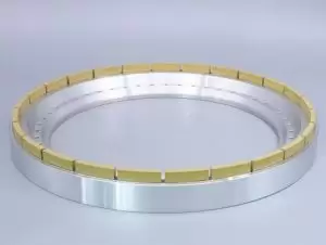
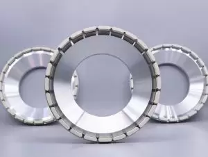
Moresuperhard diamond back Grinding Wheel for Surface Grinding Various Silicon Wafer. The back grinding wheels can be used for the Japanese ,German, American, Korean and other grinders ( Such as NTS, SHUWA, ENGIS, Okamoto , Disco, TSK and STRASBAUGH grinding machine, etc ).
—-EDITOR: Doris Hu
—-POST:Doris Hu