
Processing technology of monocrystalline silicon wafer
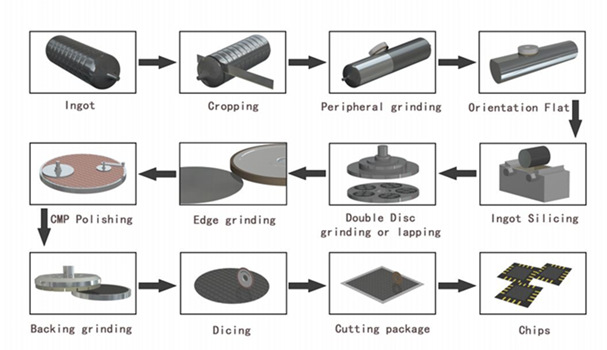
The processing technology of monocrystalline silicon wafer is mainly as follows:
* Cutting
* Cylindrical grinding ingot
* Slicing
* Chamfering
* Grinding/lapping
* Corrosion, cleaning
Moresuperhard have rich experience on providing solutions for semiconductor industry from silicon ingot cutting, slicing to final wafer product, we can provide:
* Diamond cutting blade for ingot
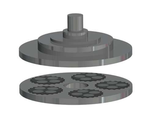
* Cylindrical grinding wheel for ingot
* Double disc grinding wheel for lapping wafer
* Metal diamond edge grinding wheel for chamfering wafer dge
* Polishing pad and polishing fluid for CMP polishing
* Back grinding wheel for wafer thinning
* Diamond hub-less /hub dicing blade
Cutting
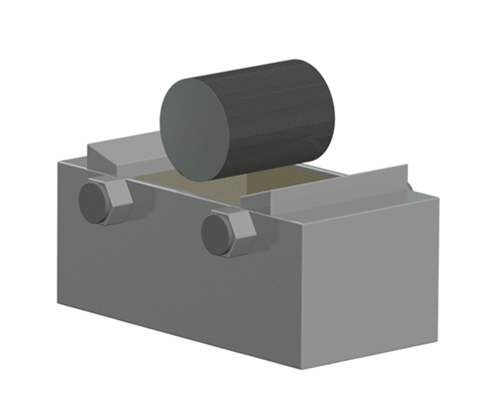
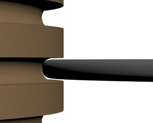
It means that after the crystal growth is completed, the useless parts of the head and tail of the crystalline silicon are cut along the direction perpendicular to the crystal growth, that is, the seed crystal and the shoulder part of the head and the ending part of the tail. Cutting is usually performed with an external circular cutting machine. The edge of the external circular cutting machine blade is diamond coated.
The blade of this cutting machine is thick, fast, and easy to operate but the blade slit is wide, wastes material and the mechanical damage on the surface of the silicon wafer is serious. At present, there are also belt cutters used to cut crystalline silicon, especially for large-diameter single-crystal silicon.
Cylindrical grinding silicon ingot:
In Czochralski single crystal silicon, due to thermal vibration, thermal shock and other reasons during crystal growth, the crystal surface is not very smooth, that is to say, the diameter of the whole single crystal silicon has a certain deviation and fluctuation; and after the crystal growth is completed There are flat ridges on the surface of single crystal silicon rods, which need to be further processed to make the diameter of the whole single crystal silicon rods uniform, so as to facilitate operation in subsequent materials and processing techniques.
Slicing :
After the single crystal silicon spheronization process is completed, it is necessary to slice the single crystal silicon rod. When slicing monocrystalline silicon for solar cells, the parameters such as the crystal orientation, parallelism and warpage of the silicon wafer are not highly required, and only the thickness of the silicon wafer needs to be controlled.
The single crystal silicon rod is cut into wafers, and the sharp edges of the wafers need to be trimmed into circular arcs, mainly to prevent the cracking of wafer edges and crystal lattice defects.
After slicing, there will be line marks on the surface of the silicon wafer. It is necessary to remove the saw marks and surface damage layer caused by the slicing through grinding, so as to effectively improve the warpage, flatness and parallelism of the single crystal silicon, and achieve a polishing process specification.
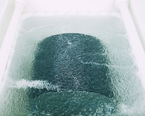
 Etching, cleaning:
After slicing, there is a mechanically damaged layer on the surface of the silicon wafer, the crystal lattice near the surface is incomplete, and the surface of the silicon wafer is polluted by impurities such as metal particles. Therefore, after generally slicing, before preparing solar cells, it is necessary to chemically etch the silicon wafer. During the processing of single crystal silicon wafers, cleaning is required in many steps, and the cleaning here is mainly the final cleaning after etching. The purpose of cleaning is to remove all sources of contamination from the wafer surface. The common cleaning method is mainly the traditional RCA wet chemical cleaning technology.
Flatness
The flatness is one of the most important parameters of the silicon wafer, mainly because the polishing process is very sensitive to the flatness of the local position, and the flatness of the silicon wafer refers to the thickness change on a straight line passing through the silicon wafer. It is obtained by the distance between the surface on the silicon wafer and a specified reference plane.
Epitaxial layer
Epitaxial layers require, in some cases, that the silicon wafer has a very pure silicon surface with the same crystal structure (single crystal) as the substrate. There is also a need to maintain control over the type and concentration of impurities. This is achieved by depositing an epitaxial layer on the silicon surface.
In the silicon epitaxy process, the silicon substrate is used as a seed crystal, and a thin layer of silicon is grown on the silicon wafer. The new epitaxial layer replicates the crystal structure of the silicon wafer. The epitaxial layer can be n-type or p-type, independent of the doping type of the original silicon wafer.
The reason for the development of silicon epitaxy is to improve the performance of bipolar devices and integrated circuits. For example, the breakdown voltage of the pn junction can be optimized while reducing the collector series resistance; in CMOS integrated circuits, the latch-up effect can be minimized.
The thickness of the epitaxial layer is typically 0.5 to 54 μm for high-speed digital circuits and 50 to 100 μm for silicon power devices.
What aspects of wafer quality are measured?
* physical size
* Flatness
* micro-roughness
* Oxygen content
* Crystal defects
* Particles
* Volume resistivity
—EDITOR: Doris Hu
—POST: Doris Hu