


Moresuperhard at CIOE 2026 | Optical & Semiconductor Solutions
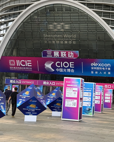
From September 9 to 11, 2026, the 27th China International Optoelectronic Exposition (CIOE 2026) was held at the Shenzhen World Exhibition & Convention Center in Shenzhen, China. As a comprehensive exhibition covering the optoelectronics industry chain, CIOE 2026 brought together technologies and products across information and communication, precision optics, laser and intelligent manufacturing, infrared, sensing, display, AR/VR and photonics innovation.
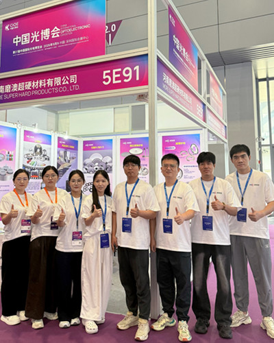
Moresuperhard participated in CIOE 2026 at Booth 5E91, focusing on the development and application of grinding and polishing consumables for optical, semiconductor and other precision materials.
For Moresuperhard, the exhibition was more than an opportunity to display products. It provided a direct view of current processing requirements across optical components, semiconductor substrates, fiber-optic components and other precision manufacturing applications.
CIOE 2026 Connected Optical and Semiconductor Manufacturing
One of the most important observations from CIOE 2026 was the close connection between optical manufacturing and semiconductor processing.
CIOE 2026 was held concurrently with the International Integrated Circuit Innovation Expo (IICIE 2026) and Shenzhen International Electronics & Embedded Systems Expo (elexcon 2026). Together, the three exhibitions created a broader platform covering optoelectronics, integrated circuits, electronics and related manufacturing technologies.
The official CIOE program also included an Optical Semiconductor Inspection Technology Forum in Hall 5, addressing advanced semiconductor manufacturing and optical inspection technologies. Other forums focused on optical ultra-precision manufacturing, meta-optics and micro-nano optical manufacturing.
Precision Optics at CIOE 2026
Precision optics was one of the major areas of interest for Moresuperhard during CIOE 2026.
The official Precision Optics Expo covered optical materials, optical components, sapphire manufacturing and applications, optical processing equipment, optical lenses, optical coating, optical measurement and related technologies.
The CIOE 2026 technical program also included dedicated discussions on precision optical technology, optical ultra-precision manufacturing, meta-optical and micro-nano optical manufacturing, as well as optical semiconductor inspection.
For manufacturers of optical components, grinding and polishing are critical processing stages because the final component performance depends not only on optical design and material selection, but also on the accuracy and surface quality achieved during manufacturing.
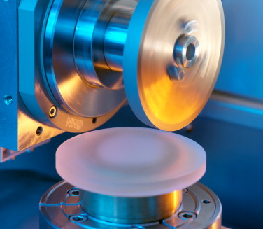
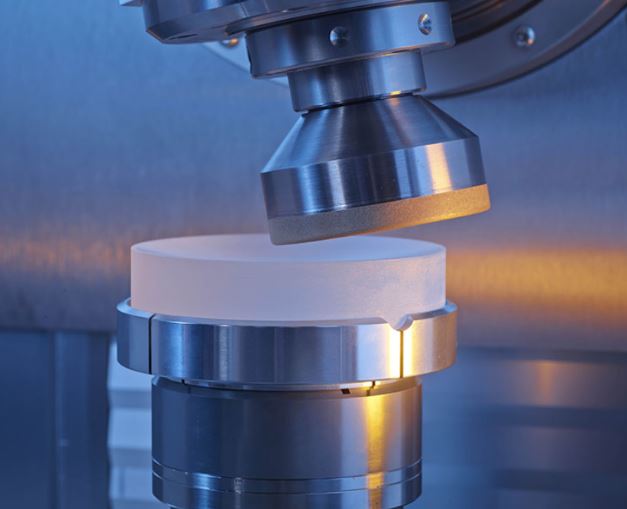
Grinding and Polishing of Optical Components
Unlike semiconductor wafer processing, optical component manufacturing is primarily concerned with generating and refining the required optical geometry, dimensional accuracy and surface finish of components such as lenses, prisms and other precision optical elements.
Depending on the component and manufacturing process, optical processing may involve rough grinding, precision grinding, fine grinding and polishing.
For optical glass and other optical materials, abrasive tools and polishing consumables need to be selected according to the material, component geometry, processing stage and required surface condition.
Moresuperhard focuses on consumables that can be integrated into different stages of this optical processing chain.
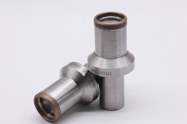
Optical Grinding Wheels for Lenses, Prisms and Optical Components
Diamond grinding wheels are widely used in precision processing of hard and brittle optical materials.
For optical components, the grinding stage is responsible for generating the required geometry and removing material before finer finishing operations. The grinding wheel therefore needs to be matched to the material and machine rather than selected only according to wheel dimensions.
Depending on the application, factors such as abrasive type, bond system, grit size, wheel structure, dimensional accuracy and machine configuration can influence grinding performance.
For lens and prism processing, the grinding solution should also be considered together with the component geometry and the subsequent polishing process.
Polishing Pads and Consumables for Optical Components
After grinding, optical components may require one or more polishing stages to achieve the required surface condition.
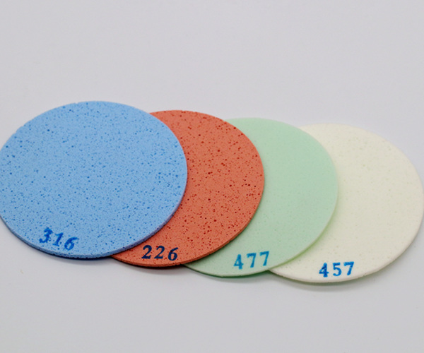
Moresuperhard provides different polishing consumables for precision surface finishing, including:
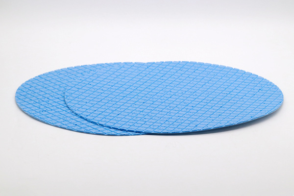
–Polyurethane polishing pads
–Diamond polishing pads
–Polishing liquids and slurries
The selection of a polishing pad should not be separated from the abrasive and process conditions. Pad hardness, structure, surface characteristics and interaction with the abrasive can affect the polishing process.
For optical applications, the target is to establish a suitable combination of component material, polishing pad, abrasive, slurry or polishing liquid, machine and processing parameters.
Semiconductor Processing at CIOE 2026
Semiconductor processing represents a separate application area from optical component manufacturing.
CIOE 2026 was held alongside the International Integrated Circuit Innovation Expo and elexcon, creating a broader platform covering optoelectronics, integrated circuits, electronics and related manufacturing technologies. The official CIOE program also included an Optical Semiconductor Inspection Technology Forum in Hall 5, addressing inspection and metrology challenges in advanced semiconductor manufacturing.
The official exhibition profile separately identifies semiconductor materials and semiconductor equipment and manufacturing within its Information and Communication Expo.
For Moresuperhard, this area is particularly relevant to precision abrasive consumables used in wafer and substrate processing.
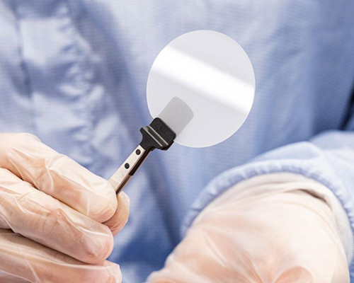
Semiconductor Grinding and Cutting Consumables
Semiconductor material processing involves a different sequence of operations from optical component polishing.
Depending on the material and manufacturing stage, processing may include dicing, wafer thinning, chamfering, grinding, lapping and polishing.
Different operations require different consumables:
* Dicing blades for wafer and substrate cutting
* Wafer thinning grinding wheels for backside grinding and thickness reduction
* Wafer chamfering wheels for wafer edge processing
* Diamond grinding wheels for precision material removal
* Lapping pads for controlled surface processing
* Polishing pads for fine surface finishing
* Diamond polishing pads for abrasive polishing applications
* CMP-related consumables for applicable semiconductor surface-finishing processes
Silicon, SiC and Sapphire Processing
Different semiconductor and optoelectronic materials require different processing strategies.
Silicon wafers require controlled cutting, grinding, thinning, edge processing and polishing throughout different stages of wafer manufacturing.
Silicon carbide (SiC) is a hard material that requires appropriate abrasive and process selection for cutting, grinding and polishing operations.
Sapphire is also used in optoelectronic applications and requires precision processing because of its material characteristics.
Although silicon, SiC and sapphire can all involve diamond abrasive processing, the consumable specification should not automatically be treated as interchangeable. Material properties, equipment and processing objectives need to be considered when selecting the grinding or polishing solution.
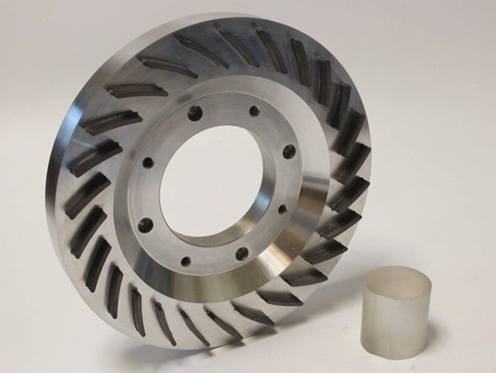
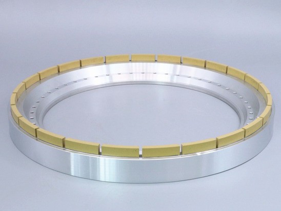
Wafer Thinning Grinding Wheels for Semiconductor Processing
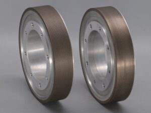
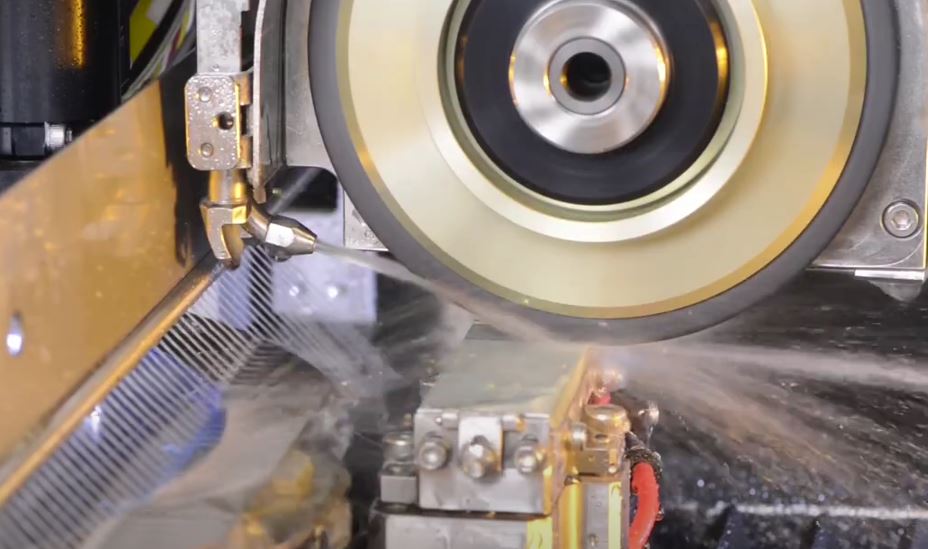
Wafer thinning is an important grinding operation in semiconductor manufacturing. The process removes material from the wafer backside to achieve the required thickness and prepare the substrate for subsequent manufacturing steps.
The grinding wheel needs to be selected according to the wafer material, equipment configuration, grinding conditions and target surface requirements.
For semiconductor applications, the objective is not simply to remove material quickly. Process stability, wafer thickness control and surface condition also need to be considered when selecting the grinding solution.
Moresuperhard therefore regards wafer thinning grinding as an application that requires the abrasive tool to be matched to the material and processing conditions rather than treated as a standard grinding-wheel application.

Wafer Chamfering Wheels for Edge Processing
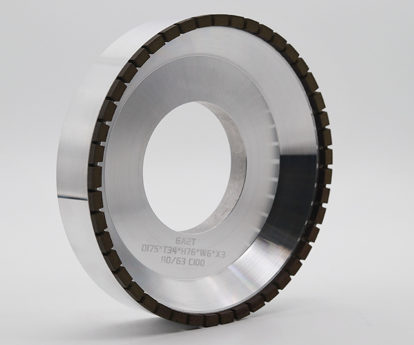
Wafer chamfering focuses on processing the wafer edge and generating the required edge geometry.
Chamfering wheels need to provide controlled material removal while maintaining consistent edge processing. Wheel specification, abrasive characteristics, dimensional accuracy and compatibility with the existing equipment all need to be considered when developing a chamfering solution.
This application is distinct from backside wafer thinning and should therefore be treated as a separate grinding process rather than simply using the same wheel specification for both operations.
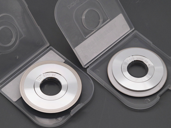
Semiconductor Dicing Blades
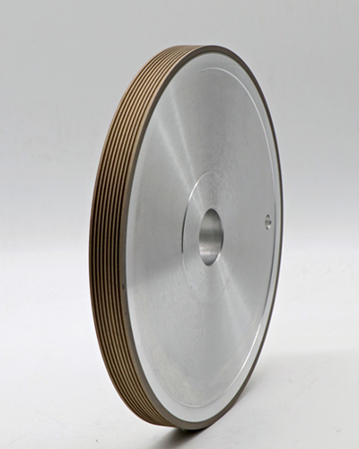
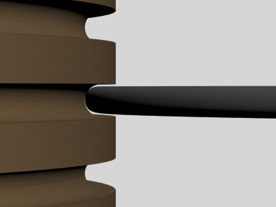
Diamond dicing blades are used to separate semiconductor wafers, substrates and other precision materials into individual components.
Blade selection depends on the material being cut, cutting equipment, required kerf, cutting conditions and the desired edge quality.
Different semiconductor and optoelectronic materials can present different cutting requirements. Silicon, compound semiconductor materials, sapphire and other hard or brittle substrates therefore require application-specific blade selection.
At CIOE 2026, discussions around cutting and dicing further demonstrated the importance of precision consumables in the early stages of semiconductor and optoelectronic manufacturing.
Semiconductor Polishing Pads
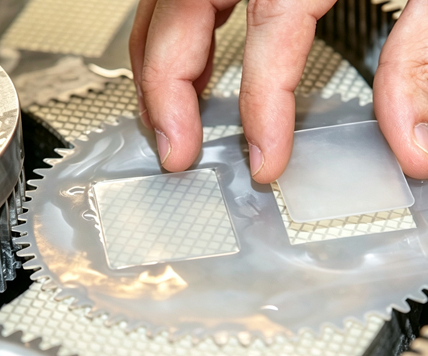
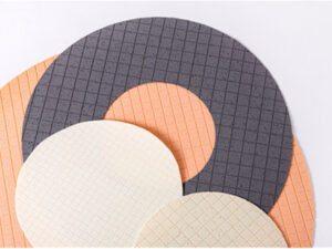
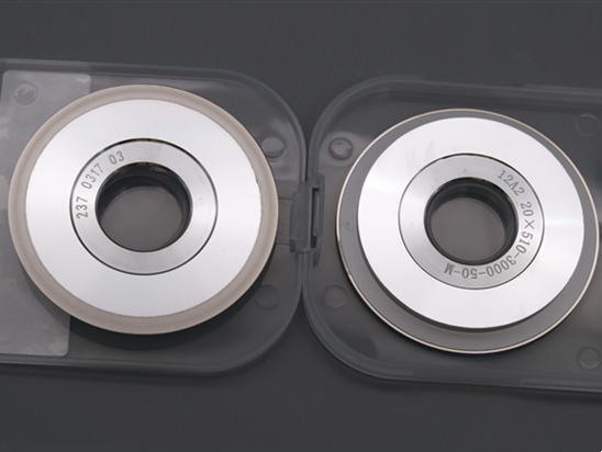
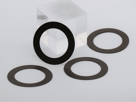
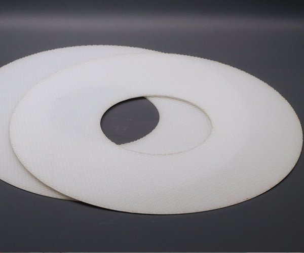
After grinding and other material-removal processes, semiconductor substrates may require lapping and polishing to achieve the required surface condition. Polishing pads play an important role in the interaction between the substrate, abrasive and polishing equipment.
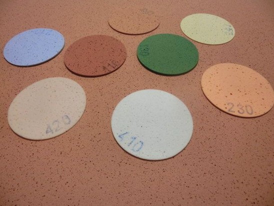
Moresuperhard supplies polishing-related consumables including polyurethane polishing pads, diamond polishing pads, lapping pads and related abrasive materials.
For semiconductor applications, pad selection should consider the material, polishing stage, slurry or abrasive system, machine configuration and target surface requirements.
Polishing pad performance depends on factors such as pad structure, hardness, compressibility, surface characteristics and interaction with the polishing slurry. Different materials and different polishing stages may therefore require different pad configurations.
Optical Processing and Semiconductor Processing Require Different Solutions
One important takeaway from CIOE 2026 is that optical component processing and semiconductor material processing should not be treated as the same application.
| Application | Optical Component Processing | Semiconductor Processing |
|---|---|---|
| Main materials | Optical glass, lenses, prisms, optical elements | Silicon, SiC, sapphire, semiconductor substrates |
| Typical focus | Optical geometry and surface finish | Thickness, edge geometry, material removal and surface condition |
| Key processes | Grinding, fine grinding, lapping, polishing | Dicing, thinning, chamfering, grinding, lapping, polishing |
| Typical consumables | Diamond grinding wheels, polishing pads, diamond abrasives, polishing films and slurries | Dicing blades, thinning wheels, chamfering wheels, grinding wheels, lapping pads and polishing pads |
This distinction is important when selecting a consumable because the same abrasive technology may be used in different industries, while the actual product specification and processing objective can be completely different.
From CIOE 2026 to Future Grinding and Polishing Solutions
CIOE 2026 provided a valuable view of the continued convergence between optics, semiconductors, precision manufacturing and advanced materials.
The official conference program included dedicated discussions on optical semiconductor inspection, optical ultra-precision manufacturing, meta-optics and micro-nano optical manufacturing. These topics reflect the industry’s continued movement toward higher precision, smaller structures, more complex materials and tighter process control.
For grinding and polishing consumable manufacturers, this development creates new requirements. Product specifications alone are no longer enough. Stable material removal, surface quality, dimensional consistency, consumable life and compatibility with the processing equipment all need to be considered as part of the overall solution.
Moresuperhard will continue to develop and supply precision grinding, lapping, polishing and cutting consumables for optical and semiconductor materials, while using direct feedback from customers, exhibitions and application projects to improve our products and process solutions.
Next:
This is already the latest article


