
How are semiconductor wafer manufactured?
A wafer is a thin silicon wafer with a thickness of about 1 mm. Due to the very high requirements of the manufacturing process, the surface of the wafer has a very high flatness. The specific application of the wafer determines which crystal growth method needs to be adopted. Taking the Czochralski method as an example, after the polysilicon is melted, a pencil-sized seed crystal is immersed in the molten silicon, and then the seed crystal is slowly rotated and slowly pulled upward. So a very heavy monocrystalline silicon ingot was pulled out. In addition, targeted electrical properties of the wafer can be achieved by adding trace amounts of high-purity dopants to the molten silicon. Ingots are doped according to customer specifications, then sliced and polished. After several steps, customers receive wafers specially packaged to their specific specifications.
CZOCHRALSKI PROCESS
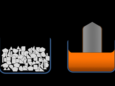
Most of the current monocrystalline silicon is crystallized by Czochralski method, which is to melt high-purity polycrystalline silicon in an ultra-pure quartz crucible and add dopants (usually boron, phosphorus, arsenic, antimony) to it. Dip the single crystal seed crystal into the molten silicon, then slowly rotate and lift it up, and gradually pull out a columnar silicon ingot with a head cone and a tail cone. Such nose and tail cones prevent dislocations caused by thermal shock.
The temperature, flow rate of molten silicon, the speed of crystal and crucible rotation, and the precise control of the pulling speed play a key role in obtaining high-quality single crystal silicon ingots.
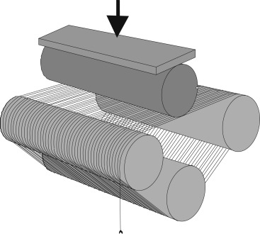
FLOAT ZONE METHOD
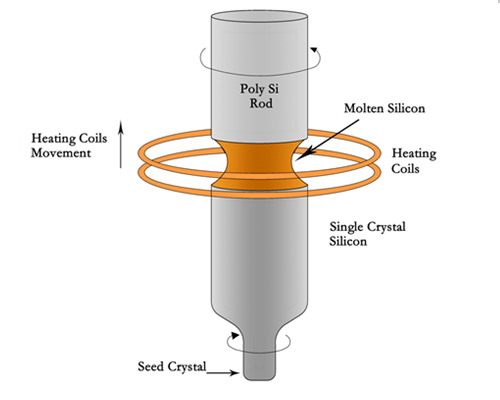
The float zone method is an ideal crystal growth method for power devices such as IGBTs.
As shown in the figure, a cylindrical polysilicon ingot is placed above an induction coil, and under the action of a wireless magnetic field, the induction coil heats and melts the ingot from the lower part of the polysilicon rod above the coil. The strength of the electromagnetic field can be adjusted. Molten silicon flows down through the small hole in the middle of the induction coil to form single crystal silicon (zone melting method). For the zone melting method, the doping is generally boron or phosphorus, and is achieved by doping its gaseous substances.
After the silicon ingot has been cut through the cutting head cone, tail cone, and quality inspection after cutting, the Czochralski or zone melting silicon wafer should go to the wafer processing stage.
These processes involve first precisely aligning the crystal segments and then grinding the segmented crystal cylinders to the desired diameter size. The last step is to add crystal orientation marks. For large-sized wafers, a groove is generally ground on the cylindrical surface as a positioning groove (Notch), and a flat edge is generally ground as a positioning edge (Flat) for small-sized wafers.
WIRE SLICING
The first step in slicing silicon segments is to use wire cutting technology, which is currently the mainstream slicing method.
A slender (up to several miles) metal wire is guided by the guide rollers (Wire Guide Rollers) and evenly distributed at very precise intervals to form a wire web (Wire Web). When the metal wire mesh is slowly pulled on the silicon segment, the cutting fluid nozzle (Slurry Nozzle) will spray cutting fluid on the wire mesh. In this way, a section of silicon can be cut into hundreds of silicon slices in one process. During this process, the process parameters of each link need to be closely monitored to ensure that the thin film has a relatively uniform thickness and that the two sides of the silicon thin film remain relatively parallel.
Monocrystalline silicon is very brittle and has a high risk of fragmentation. Therefore, special care needs to be taken during chamfering to avoid mechanical damage to the wafer edge.
The unchamfered silicon wafer is placed on the grinding chuck, and the chamfering grinding wheel with rounded grooves grinds the edge of the wafer, so that the edge of the wafer engages the groove, and is chamfered many times by grinding wheels with different abrasive grains, thus Grind the edge fillet according to the customer’s requirements. Chamfering is divided into T-type chamfering (large chamfering) and R-type chamfering (small chamfering).
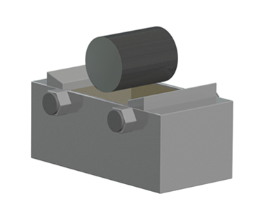
LAPPING
After the wire cutting and chamfering of the silicon wafer, the surface of the wafer needs to be ground, which can improve the parallelism of the silicon wafer surface and eliminate the surface damage caused by the wire cutting process.
During grinding, the silicon wafer is fixed on the Lapping Carrier between the upper and lower lapping plates as shown in the figure above. When the upper and lower lapping plates rotate in opposite directions, both sides of the silicon wafer can be simultaneously cleaned. Grinding effect. During the grinding process, Lapping Slurry will be continuously added, and about 10 microns of silicon will be ground off on one side during the entire grinding process.
CLEANING AND ETCHING
After mechanical processing, silicon wafers need to be cleaned and etched to eliminate residual mechanical damage on the surface. Alkaline or acidic solutions, or a mixture of both, can be used for etching. The picture above shows the Cleaning Bath, Etch Bath, and Dryer respectively.
POLISHING
The polishing process is to polish the surface of the silicon wafer to a bright mirror state and further improve the flatness of the silicon wafer (Flatness). During polishing, the silicon wafer is placed on the supporting plate, and the polishing cloth (Polishing Cloth) attached to the polishing plate (Polishing Plate) is squeezed.
Wafers with a diameter of 200mm (8 inches) and below are usually polished on one side, and wafers with a diameter of 300mm and above are mostly polished on both sides, but this is not an absolute process method, and it mostly depends on customer needs.
Similar to the aforementioned grinding process, the wafer is fixed between the upper and lower discs, and the upper and lower polishing discs simultaneously polish the front and back of the wafer. The polishing liquid and polishing pressure determine the quality and smoothness of the final polishing.