
Semiconductor die sawing
The pre-production process of semiconductor devices is usually divided into two parts: wafer manufacturing process and sealing test process. General sealing and testing processes include wafer thinning, chip placement, wafer cutting, wafer mounting, bonding, packaging, post-curing, edge removal, electroplating, printing, rib cutting and forming, appearance inspection, product testing and other procedures.
A wafer is usually composed of hundreds or tens of thousands of small chips, depending on the wafer processing process and the customer’s demand for products. In most of the wafers in the industry, there is a gap difference between Dice ranging from 40um to 100um, which is known as the scratch cutting path. However, 99% of the chips on the wafer have independent performance modules. In order to separate the small chips into single Dice, cutting and separation is required by the cutting process, which is called die sawing or wafer cutting. At present, there are two kinds of die sawing processes in the industry: laser cutting and blade cutting.
Principle of blade cutting:
Driven by the high-speed operation of the main shaft of the equipment, the diamond particles on the blade will break down the wafer on the working plate from the cutting block, and under the action of the blade and the cutting flushing water, the product debris will be removed in time, so as to avoid the abnormal quality caused by the penetration and adhesion of silicon powder on the back.
Die sawing is a very important process in semiconductor packaging process. The cutting result will directly affect the yield of the whole packaging quality. More Superhard company engaged in semiconductor die sawing production.
Application area:
Main processing silicon wafers, gallium arsenide wafers, oxide wafers and other materials。
Characteristic:
1. Stable machining performance under high load
2. By precise concentration and diamond particle adjustment, machining quality and service life can be effectively controlled
3. High stability, in the process of cutting can prevent the occurrence of broken, snake cutting, breakage and other undesirable processing phenomenon
Analysis of common anomalies for wafer cutting:
| Common anomalies | Analysis | Improvement measure |
| Chipping | 1. Incorrect blade selection
2. Unreasonable setting of machining parameters 3. Poor accuracy of equipment 4. Water temperature overhigh |
1. Select the corresponding blades for products with different results and materials
2. Optimize machining parameters 3. Correct machine accuracy 4. Control the water temperature |
| Silicon powder penetration | 1. The blade edge is narrow, the product is thick, and the film adhesive layer is strong
2. The cutting water flow is small 3. Lower spindle speed |
1. Select the appropriate blade and cutting film
2. Adjust the cutting water flow 3. High spindle speed is easy to bring out debris |
| Coil cutting | Blade strength does not match the speed | Choose the right blade and a reasonable spindle speed |
| The cut marks offset | 1. The cumulative error of the machine itself
2. Product size difference |
1. Calibrate the movement accuracy of the machine shaft
2. Accurate measurement of product dimensional accuracy |
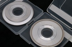
Here is a picture of electroplated wheel hub cutter
According to different wafer materials, choosing the right cutting tool can help to reduce or eliminate the damage to the edge of the product and improve the pass rate of the product. More Superhard Products Co., Ltd. is mature and stable in the manufacturing process of the dicing blades, and enjoys good stability and long life in the field of semiconductor die sawing, which is favored by the customer groups