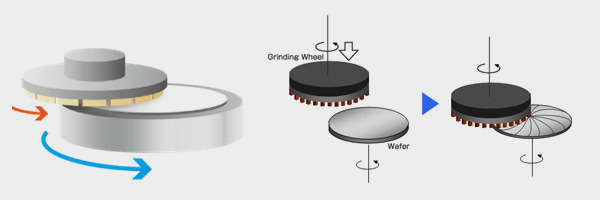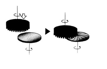
The process of backside grinding of silicon wafer
Characteristics of silicon wafer self-rotating grinding method:
1. Ductility domain grinding can be realized. When the grinding depth is less than a critical value, ductile domain grinding can be realized. A large number of tests show that the critical value of brittle – plastic conversion of Si material is about 0.06 m. The feed speed is controlled at 10m/min, and the speed of plate bearing table is 200r/min, then the cutting depth can reach 0.05m per revolution. For self-rotating grinding, formula (1) shows that for a given axial feed speed, extremely small grinding depth can be achieved if the speed of the table is high enough.
(2) High efficiency grinding can be achieved. It can be seen from formula that by simultaneously increasing the silicon wafer speed and the axial feed speed of the sand wheel, a higher material removal rate can be achieved under the condition of maintaining the same grinding depth as ordinary grinding, which is suitable for large margin grinding.
(3) The contact length, contact area and plunge Angle of the grinding wheel and the silicon wafer are constant, the grinding force is constant, and the processing state is stable, which can avoid the phenomenon of convex and collapse of the silicon wafer. Now the diameter of more than 200mm of large size silicon wafer backgrinding (backgrinding) mostly adopts the ultra-precision grinding technology based on the principle of white rotary silicon wafer grinding.
Silicon wafer back grinding is generally divided into two steps: rough grinding and fine grinding.
In the rough grinding stage, the diamond wheel with grit 46 # ~ 500 # , the axial feed speed is 100 ~ 500mm/min, and the grinding depth is generally 0.5 ~ 1mm.
The aim is to quickly remove most of the excess material (90% of the processing allowance) from the back of the silicon wafer.
In the process of fine grinding, the machining allowance is from several microns to more than ten microns. The diamond grinding wheel with grit 2000 # ~ 4000 #, and the axial feeding speed is 0.5 ~ 10mm/min.
It is mainly to eliminate the damage layer formed during rough grinding to reach the required thickness. In the fine grinding stage, the material is removed by ductility domain mode, and the surface damage of silicon wafer is significantly reduced.
The surface morphology of silicon wafer can be improved and the thickness of damaged layer can be reduced by the method of thinning combined with rough grinding and fine grinding.
Wet corrosion and polishing process can improve the surface morphology of silicon wafers and remove the mechanical damage caused by the wafer thinning. In the actual process, combined with the requirements of devices, the method of piecewise grinding and then polishing or wet corrosion can be adopted to obtain high-quality thin silicon wafers.